
Why Microvia technology?
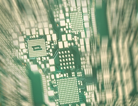
High Density Interconnect (HDI) circuit boards and microvia technology are inextricably linked. Microvias are tiny holes drilled with a laser through a thin dielectric layer. The subsequent metallisation creates a short electrical connection between two adjacent copper layers in a multilayer.
In the miniaturization of printed circuit boards, microvias, placed directly in solder pads, play a decisive role as "microvia-in-pad". "Via-in-Pad" basically means that via holes are placed directly in the solder pads, saving valuable space. Since microvias are very small blind holes, they can also be integrated into very small solder pads. The solder deposit of the solder pad fills the minimal void. Optionally, buried vias are used, which are drilled mechanically and create space for components on the placement layers.
Thin copper foils with fine and ultra-fine conductor structures are another element of HDI technology. Together with microvias, the required wiring density for complex components can also be achieved on the printed circuit board.
Advantages of Würth Elektronik HDI Microvia technologies
Anylayer Microvia technology and 50 µm structures
The key to this young technology is already in its name: Thinner layers enable even smaller microvias and thus integration into even smaller component pads. Now there is also no need for mechanically drilled vias (PTH) - any copper layer can be connected to any copper layer via very reliable microvias to save space. This also reduces the thickness of electroplated copper and makes the finest copper structures possible.
Learn more about the new possibilities here: SLIM.hdi design rules
Anylayer Microvia Technology for interposers and modules
Just like SLIM.hdi, this is an anylayer microvia technology without mechanically drilled vias. Thanks to the thin layers, the microvias can be made even smaller and integrated into extremely small component pads.
In addition, we use a special base material that is resistant to temperature cycling, with low thermal expansion and significantly reduced risk of warping and bowing. Matching the expansion behavior of silicon provides advantages when using bare dies and wire bonding technology.
Another step forward is enabled by using inkjet technology for the solder mask — our s.mask technology: BGA pitch of 0.3 mm with solder mask dams between the component pads — talk to us!
Open source smartwatch OV Tech GmbH
Together with OV Tech and its managing director Lukas Henkel, we realized a project that redefines the future of wearable electronics: an open-source smartwatch with a modular architecture.
Thanks to our ADVANCED.hdi PCB technology and the System-in-Package (SiP) approach, the smartwatch offers:
This project demonstrates how open-source concepts and high-end PCB technology can be combined to drive innovation.
Read the full success story to discover how we are pushing the boundaries of what’s possible together with OV Tech.
Relevant parameters for production-ready PCB design
Modern printed circuit board solutions are more than just connecting elements. They are the key to progress in electronics. With this in mind, we actively support our customers in development and also offer our own system solutions with electronic functions.
The HDI design rules include all the important parameters you need to make your project successful:
In our HDI design guide you will find an overview of all variants. In addition, our specialists have summarized valuable design tips for you here. This will help you bring your application to success reliably and safely.
Would you like to download our design guides and design rules as a clear technology poster? The poster provides you with the most important information about efficient PCB design.
Get started with your layout faster - thanks to standardized stackups
With these stackups, you automatically use market-standard and cost-optimized standards and avoid expensive custom builds. They also enable high-quality, cost-effective production with shorter lead times by using in-stock materials and following standardized production processes. For impedance matching stackups, please use our impedance calculation service.
Here you can find our MICROVIA.hdi standard stackups both in digital form for import into your EDA software, and as PDFs. The digital stackup files for Altium Designer contain not only the stackups but also the material data.
Here you can find our SLIM.hdi standard stackups both in digital form for import into your EDA software, and as PDFs.
Here you can find our ADVANCED.hdi standard stackups both in digital form for import into your EDA software, and as PDFs.
HDI Microvia PCBs
Here you can view or download the presentations of past HDI Microvia webinars.
"Mini, micro, microvia: HDI sample WE.microbga!"
In this webinar, learn more about our sample WE.microbga and what you can learn from it, the current design rules of the MICROVIA.hdi technology and their application, the routing of a BGA component with pitch 0.4 mm, the advantages of MICROVIA.hdi technology in terms of signal integrity and impedance calculations.
"Printed circuit board production, Part 4: High density interconnect PCBs"
Learn how the miniaturization technologies MICROVIA.hdi and SLIM.hdi are designed and manufactured and to what extent the wiring density can be increased.
"HDI Microvia - High performance printed circuit board system moves the masses"
In this webinar, we will show you how a PCB system made of HDI and printed polymer in combination with optimal thermal management meets complex requirements.
Webinar "Mini, micro, microvia: HDI sample WE.microbga!"


