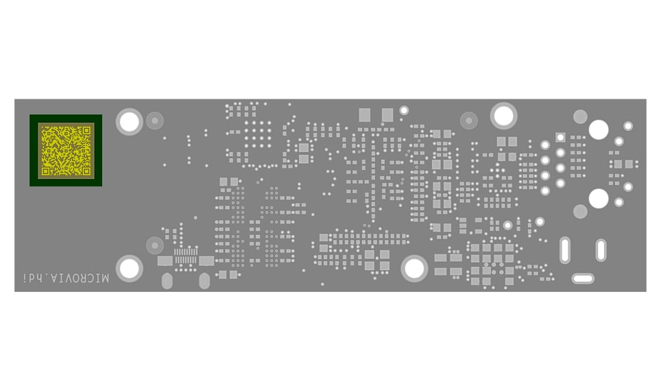
HDI microvia physical PCB sample WE.microbga
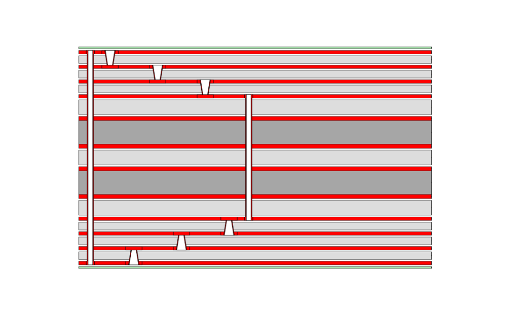
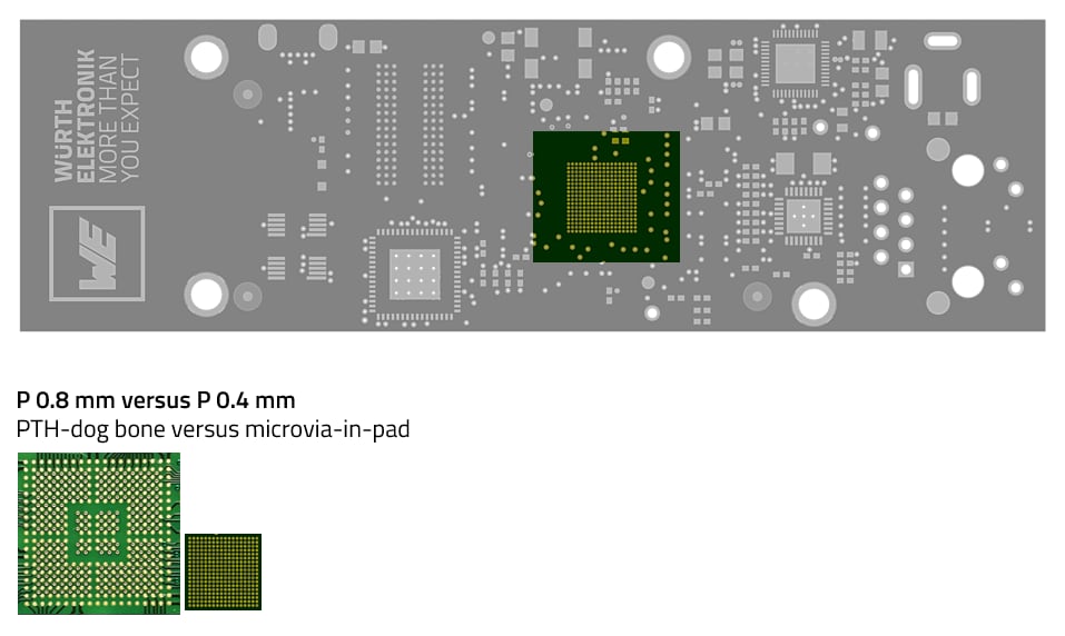
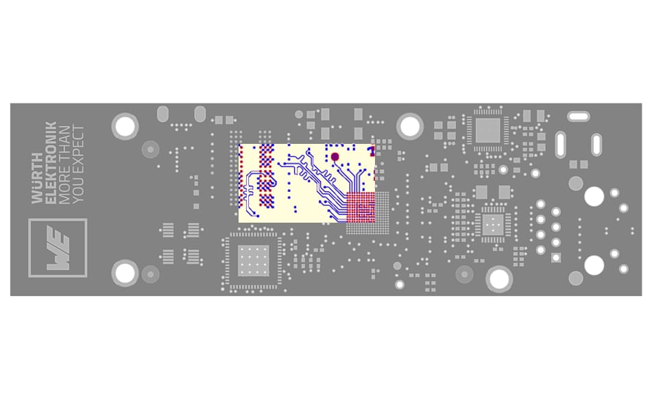
Our MICROVIA.hdi physical PCB sample WE.microbga demonstrates the power of microvia technology on rigid multilayers. Laser-drilled microvias, placed directly into the solder pads of a BGA component, can unbundle a 0.4 mm pitch to three wiring layers.
Consistently applied microvia technology offers the possibility of miniaturizing the PCB: A smaller PCB can significantly reduce the price of the PCB and also of the overall system.
At the same time, each microvia that replaces a PTH improves signal integrity by reducing parasitic effects. Other measures such as runtime matching and defined impedances through a specific stackup are demonstrated here.


