Our Capabilities
We can do it!
Modern printed circuit board solutions are more than just connecting elements. They are the key to progress in electronics. Printed circuit boards are themselves components, complex constructs made of a wide variety of materials, manufactured in a multitude of processes and with diverse functions and properties to be planned.
Würth Elektronik therefore offers standards for various PCB technologies and thus creates the basis for quality and efficiency.
Detached from all dependencies, we give you here an initial overview of the standard options and standard design parameters for materials and processes. This should not and cannot replace personal consultation. We would be happy to work with you to develop a suitable solution for your product which can also go beyond the standards shown here - please contact us!
All base materials used are IPC compliant.
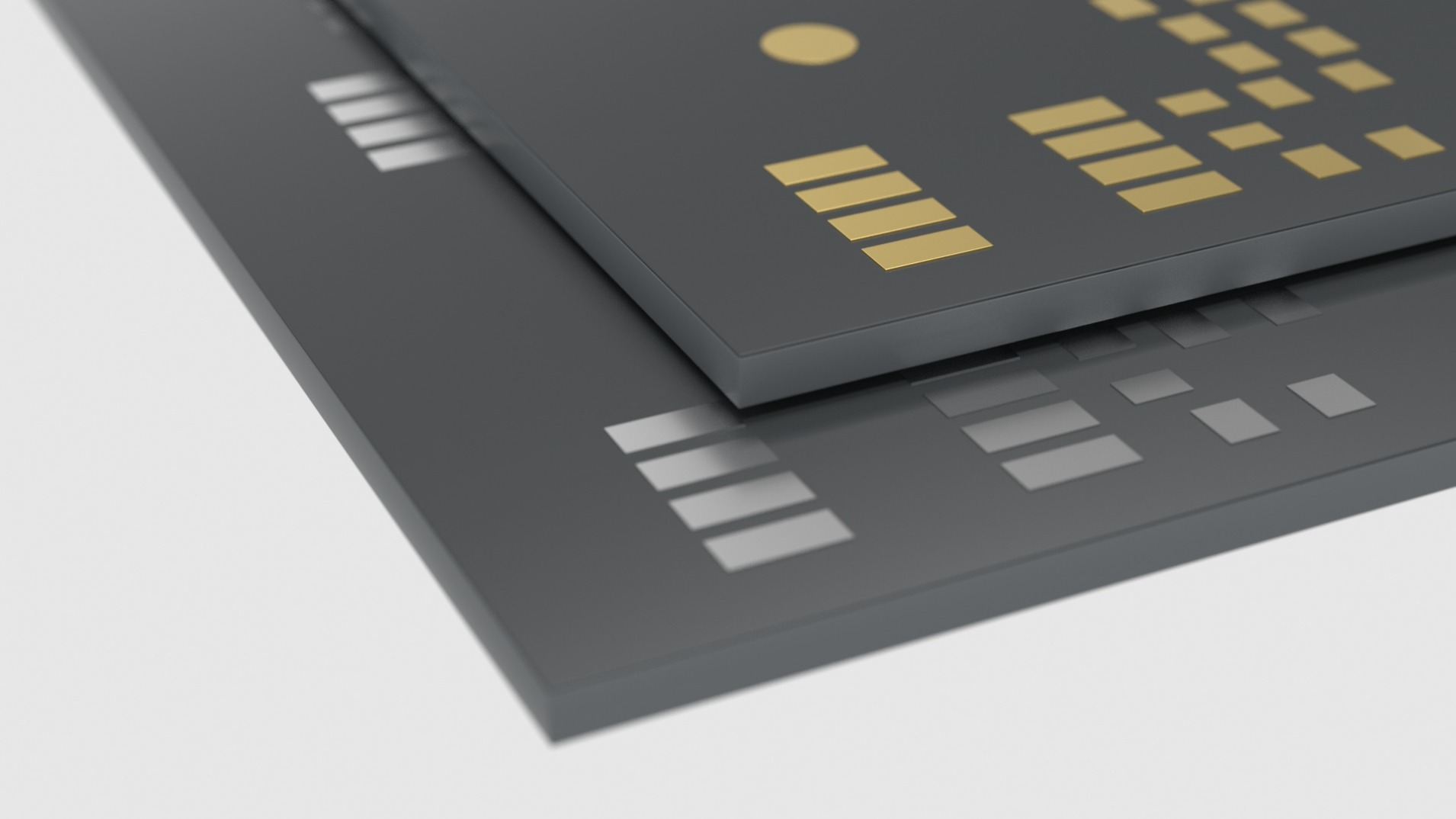
Rigid base materials are specified in IPC-4101 and its specification sheets. Standard FR-4.0 with Tg135, for example, is covered by specification sheet 21, while higher-grade FR-4.1, for example, is covered by specification sheets 128 (127) for elevated service temperatures with Tg150 and low CTE (coefficient of thermal expansion). Our portfolio is rounded off with CEM-1 materials (specification sheets 10, 15, 80) and CEM-3 materials (specification sheets 12, 14, 16, 35, 81) as well as high performance materials with higher temperature resistance or low-loss materials for high-speed / high-frequency applications (IPC-4103).
Flexible base materials are specified in the standards IPC-4202 / IPC-4203 and IPC-4204. The polyimide foils that we use are always high quality and adhesive free.
Standard copper foils according to IPC-4562.
Please contact us if you have any special requirements.
Learn more about signal integrity in our webinar recording "You have the choice: RIGID.flex with flexible soldermask or coverlay?" or in the corresponding presentation.
Standards make our lives easier, ensure the quality of products and services, and reduce costs. That's why we offer market-standard and cost-optimized standard stackups for many technologies. You can use these standards as a basis for your solutions and modify them according to your requirements.
Of course, we also manufacture according to your individual, project-specific stackups after we have checked them for technical feasibility. Please contact us!
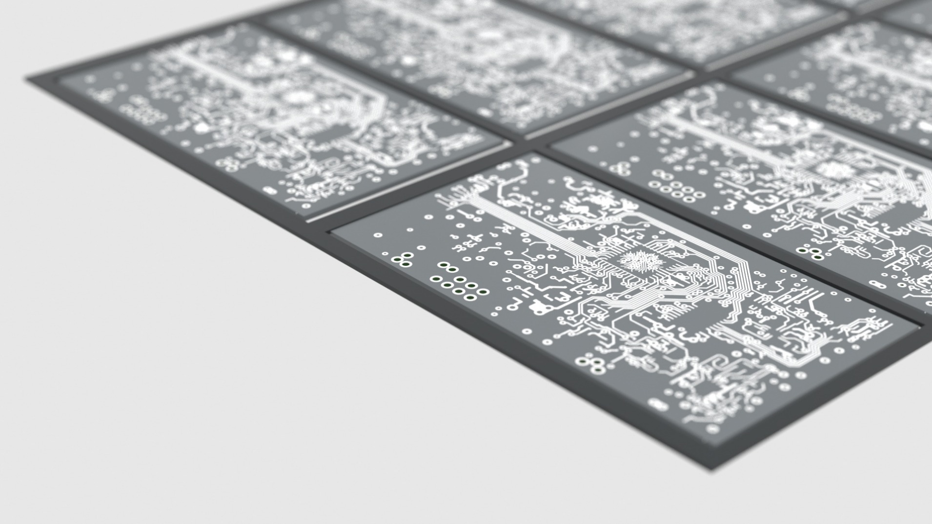
Conductor pattern structures on the inner layers are produced from the copper foil by subtractive etching. On the outer layers, conductor pattern structures consist of base copper plus copper buildup from the "through-hole plating" and "galvanic reinforcement" processes.
Depending on the copper layer thicknesses to be etched, the fineness of the structures is limited. The conductor spacing is decisive for the etching processes. The thinner the copper foils, the smaller the isolation distances can be etched. By using different values for conductor width and conductor spacing, designs can be optimized electrically and cost-wise depending on requirements.
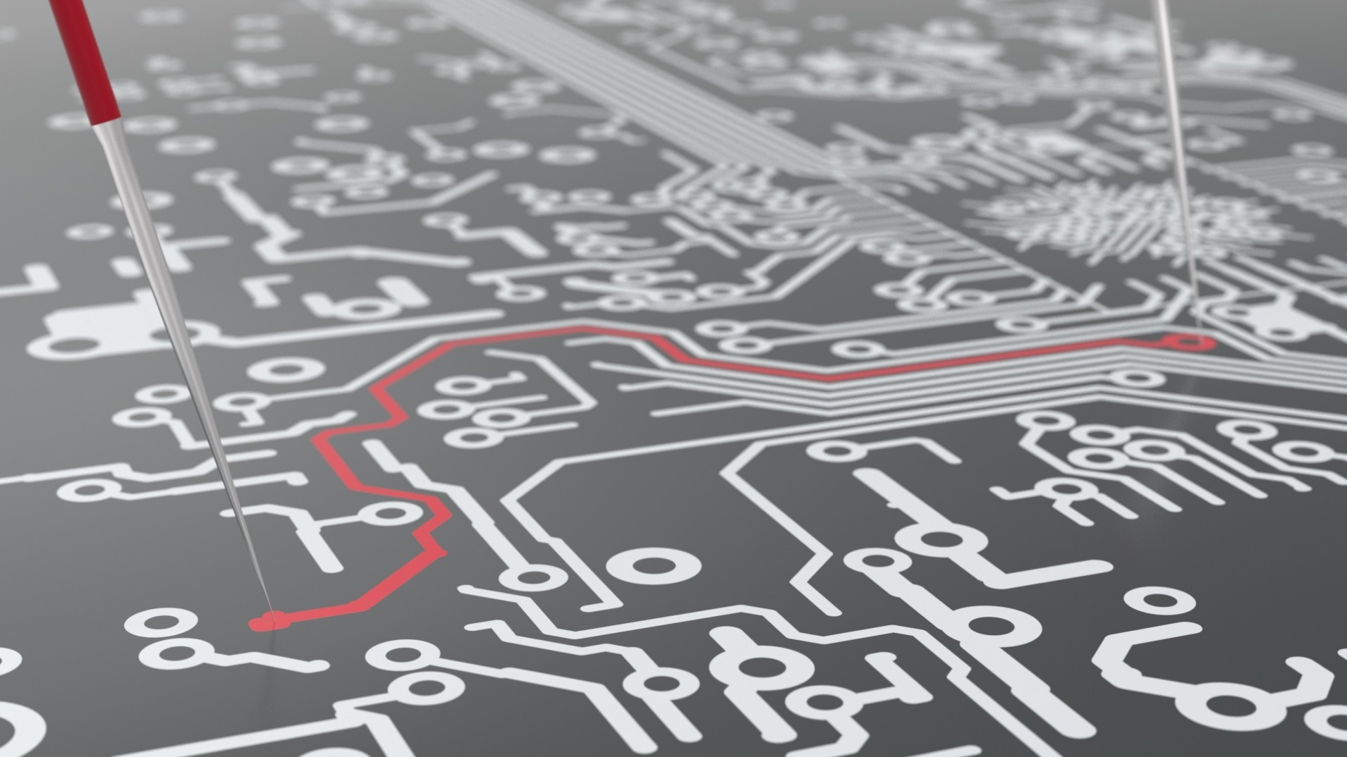
When high-speed digital signals and high-frequency analog information is routed via a printed circuit board, the transmission properties must be taken into consideration. Signal Integrity is the property of all types of printed circuit boards to distort signals only to a permissible extent so that the function of the circuit is given in the specified range. This also makes it clear that PCBs with specified Signal Integrity requirements must be custom designed: Material selection, layer structure and design rules must be coordinated and specified. We offer suitable materials (see "Base Material") and will be happy to advise you on the layer structure and definition of the design parameters. Hybrid structures are also possible.
The TDR (time domain reflectometry) impedance measurement allows to measure characteristic impedances for specified transmission lines.
You can find more information about our test procedures here.
Learn more about signal integrity in our webinar recording "Impedance is for everyone!" or in the corresponding presentation.
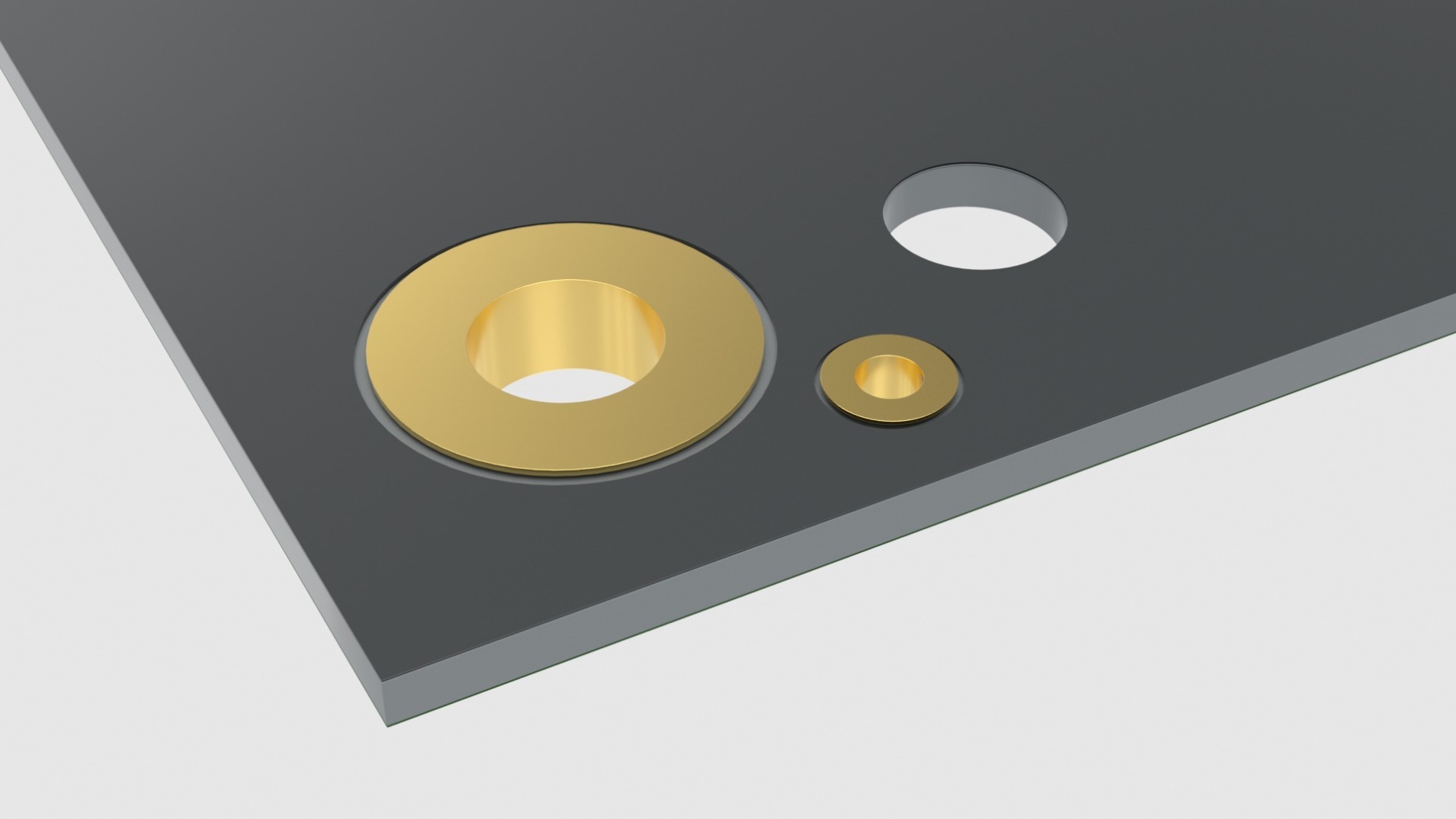
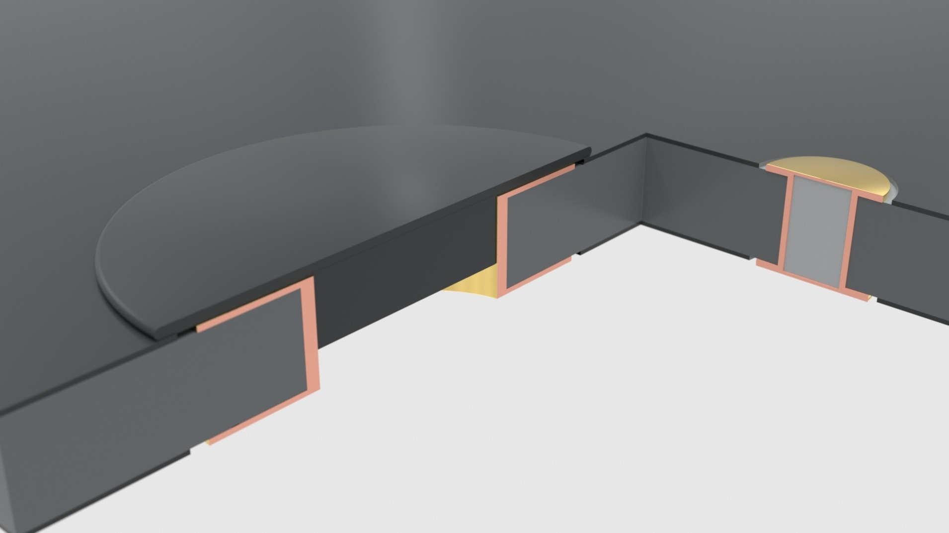
Holes can fulfill different functions. As an electrical connection between the layers of a printed circuit board, they are conductively metallized with copper. As a registration or mounting hole, the hole barrel is not metallized (NPTH = non-plated through hole). With larger diameters, PTHs also serve as mounting holes for soldering in wired components and connectors. A special feature is solderless press-fit, for which limited drill hole tolerances are necessary.
The metalization process turns mechanically drilled holes into PTHs (PTH = plated through hole), and laser-drilled holes into microvias. An important parameter in the design of holes is the ratio of hole diameter to hole depth: the aspect ratio.
For more information, please refer to our Technical Delivery Specification for printed circuit boards, chapter 3.7.1.
PTHs and microvias must have via pads for electrical contact, which are naturally much smaller on microvias and may also be integrated into the solder pads of components.
In the course of ongoing miniaturization in electronics, the requirements for via holes are also growing. They are not only used for electrical through-connection, but are also of decisive importance, for example, in terms of assembly, reliability and heat dissipation.
In our design guide "Plugging – Filling – Tenting", we have summarized not only basic definitions of terms but also the individual designs of vias with their respective objectives. So you can find the right solution for each of your use cases - within IPC-4761 and beyond.
We have summarized the most important questions and answers on this topic for you in our "Plugging & Filling" FAQs.
In the recording and the accompanying presentation of our webinar "Plugging - Filling - Tenting" you will get an insight into the linkage of PCB design with the implications for PCB manufacturing and the costs involved. We provide guidance on the general cost structure of a PCB with a view to its layout and geometry.
Our standard for solder mask is green photosensitive soldermask that meets IPC-SM-840 Class T and H requirements. Other colors such as white, black, blue, red or yellow are available upon request. Depending on the production location, the execution is as a colored solder mask instead of the green solder mask or as an additional print over the standard green solder mask.
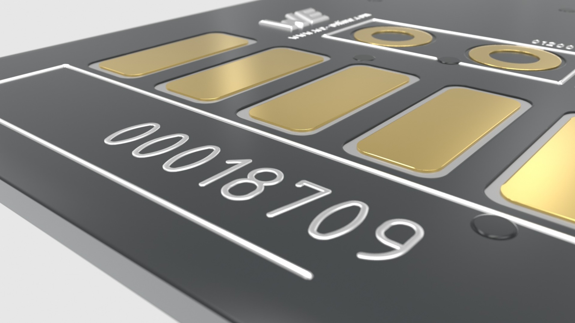
Assembly prints and markings are preferably done in white ink on solder resist, other colors are possible.
For coating, we use all commercially available technologies (screen printing, curtain coating, spraying). We already manufacture solder masks for innovative products using additive inkjet technology. For more information on this process, see the recording or the presentation of our webinar "Additive series process for flexible solder resist - our new standard".
To ensure solderability, exposed copper surfaces are coated with a solderable surface finish. More information can be found in our Technical Delivery Specification for Printed Circuit Boards, chapter 3.1.
For special requirements such as "sliding contacts", please contact us.
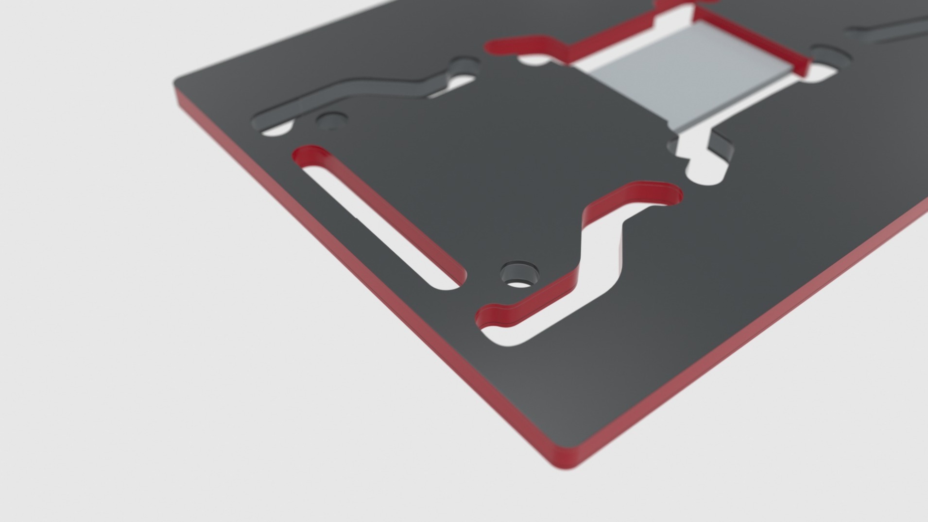
Machining of the contour of your printed circuit boards - also in the delivery panel - can be performed by v-scoring, milling or by a combination of v-scoring and milling. Flexible PCBs or flexible areas can be cut by laser.
We will be happy to support you in the design of an optimal delivery panel. Edge connectors can be chamfered. Details can be found in our Technical Delivery Specification for printed circuit boards.
For edge metalization an additional milling process is necessary before metallization.
Please refer to our Technical Delivery Specification for printed circuit boards, chapter 2.4, for the possibilities of delivery panel configuration.
By optimizing the delivery panel, our production panel can often be utilized in a better and more sustainable way, which leads to noticeable price optimizations. Please contact us.
The demands on electrical assemblies are constantly increasing. On the one hand, shorter development times for products are demanded due to cost and time pressure. On the other hand, high demands are made on the reliability of assemblies due to the operating conditions. In addition, high-quality components are used that can only be recovered at high cost and with long lead times. The printed circuit board itself also plays a decisive role in reliability. Alternative solutions must be evaluated in terms of reliability and the decisions verified by testing.
For more information on our tests methods, click here.
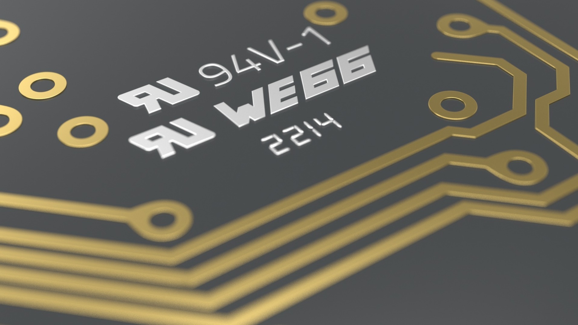
As standard we manufacture according to IPC-A-600 Class 2. Upon request, you can get class 3 both with and without test documentation. Markings according to UL standards: See chapter 1.8 of our Technical Delivery Specification for Printed Circuit Boards.
For further information on tolerances, delivery panels and certifications, please also refer to our Technical Delivery Specification for printed circuit boards.
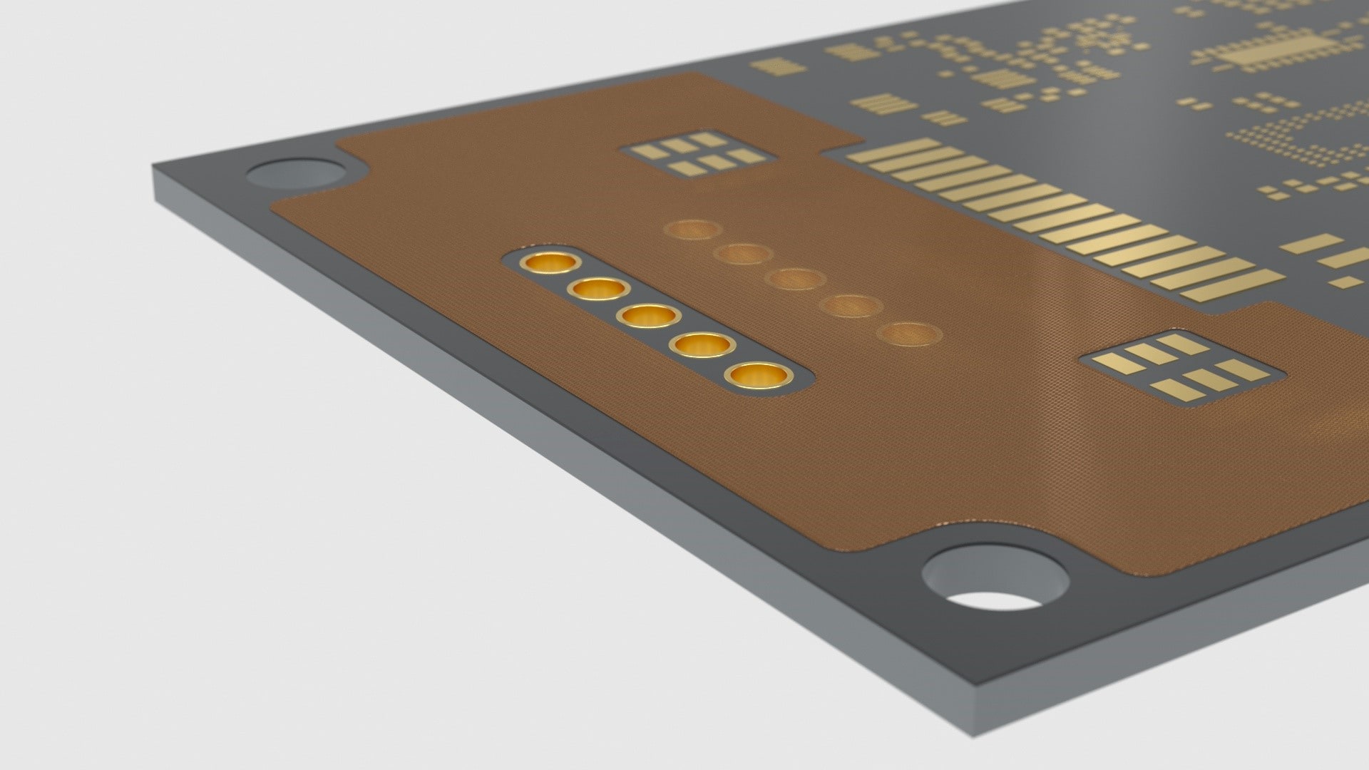
Coverlay, a composite material made of polyimide film and adhesive, can be bonded to specific areas of a printed circuit board as insulation. This allows high dielectric strength to be achieved.
You can find out which design rules have to be taken into account here.
Would you like to learn more about the use of coverlay?
Then watch the recording and presentation of our webinar "Coverlay - more than a flexible soldermask substitute" here:
Contact us


