IC-Hersteller (103)
- Alle Hersteller
 Analog Devices
 Infineon Technologies
 Microchip
 Onsemi
 Renesas
 ROHM
ROHM STMicroelectronics
 Texas Instruments
- 3peak incorporated (28)
- Ablic (23)
- Acco Semiconductor (1)
- Advanced Power (4)
- Allegro Microsystems (100)
- Alpha & Omega Semiconductor (37)
- AnalogySemi (3)
- AnDAPT Inc (204)
- Anpec (13)
- AXElite (2)
- Backward (6)
- Bright Power Semiconductor (1)
- Broadcom (46)
- Cambridge GaN Devices (18)
- Chipanalog Micro (10)
- Cologne Chips (1)
- Convenient Power (1)
- Dialog Semiconductor (12)
- Diodes Incorporated (259)
- Divimath (8)
- Elmos AG (1)
- EPC (140)
- e-Peas Semiconductors (1)
- Eta Solutions Co. Ltd. (9)
- GaN Systems (8)
- GaNPower (3)
- Giantec (1)
- Gstek Wuxi (1)
- Helix Semiconductor (7)
- IKON (1)
- Indie Semiconductor (8)
- Innovision Semiconductor Inc (2)
- Intel (68)
- Inventchip Technology (3)
- ISSI (51)
- JoulWatt (20)
- KDPOF (3)
- Kinetic Technology (8)
- Lattice semiconductor Corporation (38)
- Littelfuse (1)
- Lumissil Microsystems (8)
- M3 Technology (M3Tek) (7)
- Macnica (22)
- Marvell Semiconductor (1)
- MaxLinear (181)
- Menlo Micro (1)
- MikroE (25)
- MindCet (2)
- Monolithic Power Systems (980)
- Navitas Semiconductor Inc (6)
- NewEdge Technologies, Inc. (1)
- Nexperia (267)
- Nisshinbo Micro Device Inc. (10)
- Novosense Micro (1)
- NXP (337)
- O2 Micro International Ltd (10)
- On Bright (7)
- Panasonic (2)
- PN Junction Semiconductor (2)
- Power Integrations (117)
- Powermat (1)
- Pulsiv (19)
- Qorvo (97)
- Realsil SuRealsil(tek) Microelectronics (1)
- Richtek (297)
- Sanken Electric Co., Ltd. (16)
- Sckipio (6)
- Semtech (86)
- SG-Micro (58)
- SiFive (2)
- Silanna Semiconductor (9)
- Silergy Corporation (33)
- Silicon Laboratory Inc. (108)
- Silicontent Technology (59)
- Silvertel (59)
- Skycore Semiconductors (1)
- Skyworks (33)
- Southchip (14)
- Summit Wireless (1)
- Tagore Tech (7)
- Taiwan Semiconductor (1)
- TDK Corporation (1)
- Tempo Semiconductor (1)
- Torex (37)
- Toshiba (25)
- Transphorm (21)
- TransSIP (2)
- Union (21)
- uPI Semiconductor (2)
- Valens Semiconductor (31)
- Wise Integration (3)
- Wolfspeed (23)
- Xilinx (22)
- XL Semiconductor (3)
- XYSemi (62)
Details
| Topologie | Aufwärtswandler |
| Schaltfrequenz | 800 kHz |
| IC-Revision | 2012.12.28 |
Beschreibung
Altera Cyclone& 174; V 28 nm FPGAs provide the industry's lowest system cost and power, along with performance levels that make the device family ideal for differentiating your high-volume applications. You'll get up to 40 percent lower total power compared with the previous generation, efficient logic integration capabilities, integrated transceiver variants, and SoC FPGA variants with an ARM-based hard processor system (HPS). The family comes in six targeted variants: Cyclone V E FPGA with logic only Cyclone V GX FPGA with 3.125-Gbps transceivers Cyclone V GT FPGA with 5-Gbps transceivers Cyclone V SE SoC FPGA with ARM-based HPS and logic Cyclone V SX SoC FPGA with ARM-based HPS and 3.125-Gbps transceivers Cyclone V ST SoC FPGA with ARM-based HPS and 5-Gbps transceivers
Eigenschaften
- TSMC's 28-nm low-power (28LP) process technology
- 1.1 V core voltage
- Wirebond low-halogen packages
- Multiple device densities with compatible package footprints for seamless migrationbetween different device densities
- RoHS-compliant optionsEnhanced 8-input ALM with four registers
- M10K—10-kilobits (Kb) memory blocks with soft error correction code (ECC)
- Memory logic array block (MLAB)—640-bit distributed LUTRAM where you canuse up to 25% of the ALMs as MLAB memory
- Native support for up to three signal processing precision levels(three 9 x 9, two 18 x 18, or one 27 x 27 multiplier) in the samevariable-precision DSP block
- 64-bit accumulator and cascade
- Embedded internal coefficient memory
- Preadder/subtractor for improved efficiencyDDR3, DDR2, and LPDDR2 with 16 and 32 bit ECC supportPCI Express® (PCIe®) Gen2 and Gen1 (x1, x2, or x4) hard IP withmultifunction support, endpoint, and root port
- Up to 550 MHz global clock network
- Global, quadrant, and peripheral clock networks
- Clock networks that are not used can be powered down to reduce dynamic power
- Precision clock synthesis, clock delay compensation, and zero delay buffering (ZDB)
- Integer mode and fractional mode
- 875 megabits per second (Mbps) LVDS receiver and 840 Mbps LVDS transmitter
- 400 MHz/800 Mbps external memory interface
- On-chip termination (OCT)
- 3.3 V support with up to 16 mA drive strength
- 614 Mbps to 5.0 Gbps integrated transceiver speed
- Transmit pre-emphasis and receiver equalization
- Dynamic partial reconfiguration of individual channels
- Single or dual-core ARM Cortex-A9 MPCore processor-up to 800 MHz maximumfrequency with support for symmetric and asymmetric multiprocessing
- Interface peripherals—10/100/1000 Ethernet media access control (EMAC), USB 2.0On-The-GO (OTG) controller, quad serial peripheral interface (QSPI) flash controller,NANDflash controller, Secure Digital/MultiMediaCard (SD/MMC) controller, UART,controller area network (CAN), serial peripheral interface (SPI), I2C interface, andup to 85 HPS GPIO interfaces
- System peripherals—general-purpose timers, watchdog timers, direct memory access(DMA) controller, FPGA configuration manager, and clock and reset managers
- On-chip RAM and boot ROM
- HPS–FPGA bridges—include the FPGA-to-HPS, HPS-to-FPGA, and lightweightHPS-to-FPGA bridges that allow the FPGA fabric to issue transactions to slaves inthe HPS, and vice versa
- FPGA-to-HPS SDRAM controller subsystem—provides a configurable interface tothe multiport front end (MPFE) of the HPS SDRAM controller
- ARM CoreSight™ JTAG debug access port, trace port, and on-chip trace storage
- Tamper protection—comprehensive design protection to protect your valuable IPinvestments
- Enhanced advanced encryption standard (AES) design security features
- CvP
- Partial and dynamic reconfiguration of the FPGA
- Active serial (AS) x1 and x4, passive serial (PS), JTAG, and fast passive parallel (FPP)x8 and x16 configuration options
Weiterführende Informationen
Artikeldaten
Artikel Nr. | Datenblatt | Simulation | Downloads | Status | Produktserie | L(µH) | IR 1(mA) | ISAT(A) | RDC(mΩ) | fres(MHz) | H(mm) | B(mm) | IR(A) | Montageart | IRP,40K(A) | ISAT,10%(A) | ISAT,30%(A) | Material | Z @ 100 MHz(Ω) | Zmax(Ω) | Testbedingung Zmax | IR 2(mA) | RDC max.(mΩ) | Typ | Muster | |
|---|---|---|---|---|---|---|---|---|---|---|---|---|---|---|---|---|---|---|---|---|---|---|---|---|---|---|
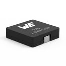 | WE-HCI SMT-Hochstrominduktivität, 1 µH, – | Status Aktivi| Produktion ist aktiv. Erwartete Lebenszeit: >10 Jahre. | ProduktserieWE-HCI SMT-Hochstrominduktivität | Induktivität1 µH | – | – | Gleichstromwiderstand4.6 mΩ | Eigenresonanzfrequenz85 MHz | Höhe3.8 mm | Breite6.9 mm | – | MontageartSMT | Performance Nennstrom16.8 A | Sättigungsstrom 18 A | Sättigungsstrom @ 30%19 A | MaterialSuperflux | – | – | – | – | Gleichstromwiderstand4.6 mΩ | – | ||||
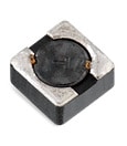 | WE-TPC SMT-Speicherdrossel, 4.7 µH, – | Status Aktivi| Produktion ist aktiv. Erwartete Lebenszeit: >10 Jahre. | ProduktserieWE-TPC SMT-Speicherdrossel | Induktivität4.7 µH | – | Sättigungsstrom1.95 A | – | Eigenresonanzfrequenz40 MHz | Höhe2.8 mm | Breite5.8 mm | Nennstrom2.4 A | MontageartSMT | – | – | – | – | – | – | – | – | Gleichstromwiderstand38 mΩ | – | ||||
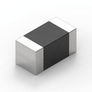 | WE-PMI Power-Multilayer-Induktivität, 10 µH, 600 mA | Status Aktivi| Produktion ist aktiv. Erwartete Lebenszeit: >10 Jahre. | ProduktserieWE-PMI Power-Multilayer-Induktivität | Induktivität10 µH | Nennstrom 1600 mA | Sättigungsstrom0.125 A | Gleichstromwiderstand300 mΩ | Eigenresonanzfrequenz20 MHz | Höhe0.8 mm | Breite2 mm | – | MontageartSMT | – | – | – | – | – | – | – | Nennstrom 2850 mA | Gleichstromwiderstand390 mΩ | TypHoher Sättigungsstrom | ||||
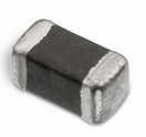 | WE-CBF SMT-Ferrit, –, 2000 mA | Status Aktivi| Produktion ist aktiv. Erwartete Lebenszeit: >10 Jahre. | ProduktserieWE-CBF SMT-Ferrit | – | Nennstrom 12000 mA | – | – | – | Höhe0.8 mm | Breite0.8 mm | Nennstrom2 A | MontageartSMT | – | – | – | – | Impedanz @ 100 MHz30 Ω | Maximale Impedanz40 Ω | Maximale Impedanz1000 MHz | Nennstrom 23000 mA | Gleichstromwiderstand40 mΩ | TypHochstrom |