Chip Antenna
Radio Module
A radio module with the appropriate radio protocol can be selected depending on the requirements for frequency, range, environmental conditions, data rates and available electrical power.
UMRF Connector
UMRF connectors offer electromechanical connections between PCBs in a small constricted space, efficient matching and EoL testing of the rod antenna.
Matching Circuit
The RF-inductors and -capacitors together build a matching circuit. Combining a Pi- and T-circuit in the PCB layout creates beneficial conditions for matching the chip antenna to possible influencing factors.
Do you need advice on selecting a matching circuit? Then visit our Design and Solution Service Antenna Matching.
Antenna
Due to their miniaturization, chip antennas can be ideally implemented in applications with limited constricted space. The implementation is most reliable when the design tips are followed.
IC Peripherals
Radio communication is implemented in the standard firmware of the radio modules, but not the final application. Applications therefore require an IC, for example a microcontroller, which requests sensor data and controls the radio module that transmits it.
Radio Module
Consider the recommended circuit and the PCB layout of the antenna feed line from the radio module data sheet.
UMRF Connector
Provide the footprint for a WR-UMRF connector on the feed line of the antenna immediately after the circuit of the radio module.
Antenna feed line
Design the feed line of the antenna to the impedance of 50 Ohm.
Keep the feed line of the antenna as short as possible.
Matching Circuit
Consider the recommended PCB layout for the matching circuit from the antenna data sheet.
Place the matching circuit as close as possible to the antenna and connect it to the radio module ground plane.
Design the matching circuit for component size 0402.
Antenna
Consider the recommended PCB layout for the antenna from the antenna data sheet.
Cut out the copper in all PCB layers under the antenna.
Place electrical antennas separated from the rest of the circuit and components.
Place magnetic antennas as centrally as possible at the edge of the longer PCB side.
Do not place any electroconductive planes, metals and batteries/accumulators in the immediate environment of the antenna.
Maximize the distance of the antenna to dielectric materials (e.g. casing).
Optional: Signal Filters
Harmonics, known as spurious emissions in radio measurements, can be attenuated with bandpass and lowpass filters.
Short Introduction to Chip Antenna
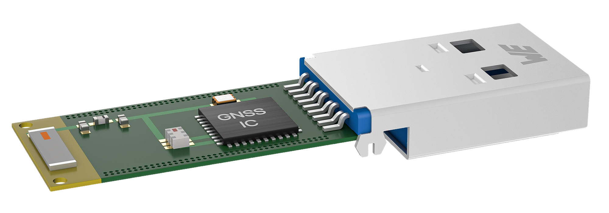
The overview shows typical components for the design of radio interfaces with chip antennas. This includes a chip antenna, matching network and UMRF connector, as well as a radio module.
The generated near-field by the integrated chip antenna is significantly influenced by the immediate environment. The main influencing factors are metals, batteries/accumulators, casings and human bodies. The position of the chip antenna on the PCB and the PCB size/geometry may significantly influence the antenna characteristics. The PCB interacts together with the chip antenna and combined they form the radiating structure.
Depending on the application, the chip antenna may be out of tune by the influencing factors and the PCB configuration. With the help of RF inductors and RF capacitors, which form a matching network, the chip antenna can be matched to the required frequency range.
Our Range of Services for Radio Modules and Antennas
Do you use our radio modules or antennas and would like technical advice? Then visit our Design and Solution Services:
Service Antenna Matching
Support Wireless Connectivity & Sensors


