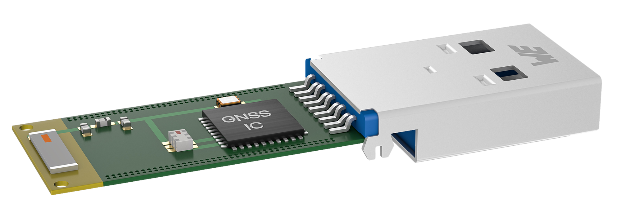
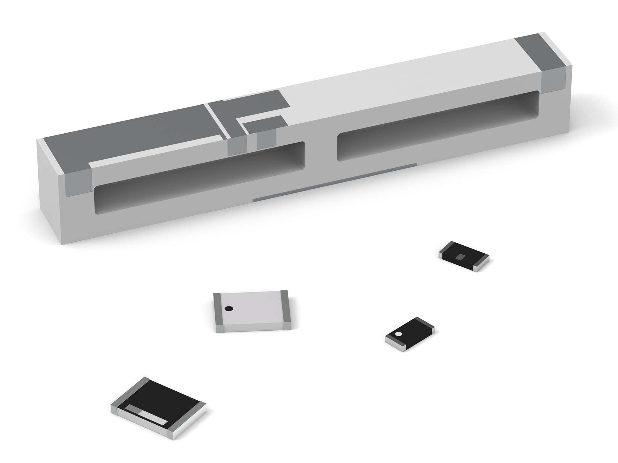
Our product portfolio includes the necessary radio modules, RF components and connectors that are required for the assembly of a radio interface.
In addition to chip antennas, rod antennas and radio modules, we offer our customers a development support service Antenna Matching. This service provides expert advice on antenna selection, placement and matching.
We look forward to hearing from you!
Antennas transmit and receive radio signals by converting electromagnetic conducted waves into free space waves and free space waves into conducted waves. In the process, an antenna forms electric and magnetic fields. The generated near field is influenced by the immediate environment. The main influencing factors are metals, batteries/accumulators, casings and human bodies. The position of the chip antenna on the PCB and the PCB size/geometry also affect the near fields, since the PCB together with the chip antenna creates the structure that operates as an antenna
Due to the influencing factors, the frequency range at which the chip antenna can transmit and receive may be out of tune. With the help of RF inductors and RF capacitors, the chip antenna can be matched to the required frequency range.
The RF inductors and RF capacitors build a matching circuit that match the impedance of the chip antenna to the required frequency range under the influence of the immediate environment. Therefore, it is necessary to make an antenna match as soon as the chip antenna, the immediate environment, the required frequency range, the position of the chip antenna on the PCB or the PCB size/geometry changes. The specified antenna performance requires the correct implementation of the chip antenna for the application. More about this in our antenna design-in guidance.
When designing a radio interface, a distinction is made between an integrated chip antenna and an external rod antenna. Visit our RF & Wireless Communication App Guide to learn more about component selection.
These recommendations form the basis for implementing our chip antennas according to the specified antenna performance in the application:
For more information, please refer to our Application Notes and Design Guides:
ANP057: WE-MCA Multilayer Chip Antenna Placement & Matching
ANP074: Introduction to RF inductors
ANE012: Coaxial PCB Connector - PCB-Transmission Line Design Guide
Our services range from antenna selection to documentation of the implemented matched antenna:
Our process enables transparent integration into your project plan. If you have any questions about the process or general questions about antenna matching, our service is also available to you.
1. Get in touch with us via the online contact form.
2. We review your information and get back to you.
3. Please have the following data ready for analysis:
4. We analyze your data and advise you.
5. After successful analysis, the following materials will be required for antenna matching:
6. We match your antenna and send you a report.
7. Your material will be returned.
Note:
Please note that your submitted materials will be manipulated for antenna matching and laboratory tests. Manipulation may include making holes and slots in the casing and soldering a cable on the antenna feed line on the PCB. The antenna feed line on the submitted PCB will be cut, therefore the antenna can no longer be controlled by the radio module. Antenna matching, laboratory testing, and manipulation may damage or destroy your submitted materials.


