IC manufacturers (105)
- All manufacturers
 Analog Devices
 Infineon Technologies
 Microchip
 Onsemi
 Renesas
 ROHM
ROHM STMicroelectronics
 Texas Instruments
- 3peak incorporated (35)
- Ablic (23)
- Acco Semiconductor (1)
- Advanced Power (4)
- Allegro Microsystems (100)
- Alpha & Omega Semiconductor (37)
- AnalogySemi (3)
- AnDAPT Inc (204)
- Anpec (13)
- AXElite (2)
- Backward (6)
- Bright Power Semiconductor (1)
- Broadcom (46)
- Cambridge GaN Devices (18)
- Chipanalog Micro (10)
- Cologne Chips (1)
- Convenient Power (1)
- Dialog Semiconductor (12)
- Diodes Incorporated (257)
- Divimath (8)
- Elmos AG (1)
- EPC (146)
- e-Peas Semiconductors (1)
- Eta Solutions Co. Ltd. (9)
- GaN Systems (8)
- GaNPower (3)
- Giantec (1)
- Gstek Wuxi (1)
- Helix Semiconductor (7)
- IKON (1)
- Indie Semiconductor (8)
- Innovision Semiconductor Inc (2)
- Intel (68)
- Inventchip Technology (3)
- ISSI (51)
- JoulWatt (20)
- KDPOF (3)
- Kinetic Technology (8)
- Lattice semiconductor Corporation (38)
- Littelfuse (1)
- Lumissil Microsystems (8)
- M3 Technology (M3Tek) (7)
- Macnica (22)
- Marvell Semiconductor (1)
- MaxLinear (181)
- Menlo Micro (1)
- MikroE (25)
- MindCet (2)
- Monolithic Power Systems (982)
- Navitas Semiconductor Inc (6)
- NewEdge Technologies, Inc. (1)
- Nexperia (268)
- Nisshinbo Micro Device Inc. (10)
- Nordic Semiconductor (1)
- Novosense Micro (1)
- NXP (341)
- O2 Micro International Ltd (10)
- On Bright (7)
- Panasonic (2)
- PN Junction Semiconductor (2)
- Power Integrations (117)
- Powermat (1)
- Pulsiv (19)
- Qorvo (99)
- Realsil SuRealsil(tek) Microelectronics (1)
- Richtek (297)
- Sanken Electric Co., Ltd. (16)
- Sckipio (6)
- Semtech (86)
- SG-Micro (58)
- SiFive (2)
- Silanna Semiconductor (9)
- Silergy Corporation (34)
- Silicon Laboratory Inc. (108)
- Silicontent Technology (59)
- Silvertel (59)
- Skycore Semiconductors (1)
- Skyworks (33)
- Southchip (18)
- Summit Wireless (1)
- Tagore Tech (7)
- Taiwan Semiconductor (1)
- TDK Corporation (1)
- Tempo Semiconductor (1)
- Torex (37)
- Toshiba (27)
- Transphorm (21)
- TransSIP (2)
- Union (21)
- uPI Semiconductor (2)
- Valens Semiconductor (31)
- VisIC (1)
- Wise Integration (3)
- Wolfspeed (23)
- Xilinx (22)
- XL Semiconductor (3)
- XYSemi (62)
Overview
| Topology | Other Topology |
| IC revision | D |
Description
The RF signal of the CN0551 is first passed through a surface acoustic wave (SAW) filter before going through the gain stages, which helps eliminate unwanted out-of-band amplification. When selecting a filter, a balance must be struck between the band flatness and the out-of-band rejection. SAW filters are also a source of insertion loss, which reduces the overall gain of the signal chain and needs to be considered during selection.In this reference design, the SAW filter used has a typical maximum insertion loss of 2 dB and a terminating impedance of 50 Ω.The CN0551 uses two amplifier stages in its RF signal path. The first stage is an AD8353 RF gain block amplifier that provides a fixed gain of 19.6 dB (Typical) in the 433.92 MHz ISM band. The AD8353 is capable of operating from 1 MHz to 2.7 GHz, and exhibits a return loss of greater than 10 dB over this entire frequency range.The RF pins of the AD8353 are internally matched to 50 Ω, allowing it to be integrated directly into standard RF signal paths without external matching networks. As shown in Figure 2, only dc blocking capacitors on the RF pins and bypass capacitors on the supply pins are required for proper operation of the AD8353. Table 1 shows the recommended values for these capacitors.
Features
- +35 dB Gain
- 433 MHz ISM Band Optimized
- 50 Ohm Input and Output Impedance Matched
- Over temperature Monitoring
- Automatic Thermal Shutoff & Turn on
Typical applications
- Medical
- Industrial Equipment
- Telecom, Datacom (Optical Modules)
- Battery Powered System
More information
Products
Order Code | Datasheet | Simulation | Downloads | Status | Product series | C | Tol. C | VR(V (DC)) | Size | Operating Temperature | DF(%) | RISO | Ceramic Type | L(mm) | W(mm) | H(mm) | Fl(mm) | Packaging | Ingress Protection Code | PCB Thickness(mm) | Center Contact | SamplesAvailability & Sample | ||||||||||||||||||||||||||||||||||||||||||||||||||||||||||||||||||||||||||||||||||||||||||||||||||||||||||||||||||||||||||||||||||||||||||||||||||||||||||||||||||||||||||||||||||||||||||||||||||||||||||||||||||||||||||||||||||||||||||||||||||||||||||||||||||||||||||||||||||||||||||||||||||||||||||||||||||||||||||||||||||||||||||||||||||||||||||||||||||||||||||||||||||||||||||||||||||||||||||||||||||||||||||||||||||||||||||||||||||||||||||||||||||||||||||||||||||||||||||||||||||||||||||||||||||||||||||||||||||||||||||||||||||||||||||||||||||||||||||||||||||||||||||||||||||||||||||||||||||||||||||||||||||||||||||||||||||||||||||||||||||||||||||||||||||||||||||||||||||||||||||||||||||||||||||||||||||||||||||||||||||||||||||||||||||||||||||||||||||||||||||||||||||||||||||||||||||||||||||||||||||||||||||||||||||||||||||||||||||||||||||||||||||||||||||||||||||||||||||||||||||||||||||||||||||||||||||||||||||||||||||||||||||||||||||||||||||||||||||||||||||||||||||||||||
|---|---|---|---|---|---|---|---|---|---|---|---|---|---|---|---|---|---|---|---|---|---|---|---|---|---|---|---|---|---|---|---|---|---|---|---|---|---|---|---|---|---|---|---|---|---|---|---|---|---|---|---|---|---|---|---|---|---|---|---|---|---|---|---|---|---|---|---|---|---|---|---|---|---|---|---|---|---|---|---|---|---|---|---|---|---|---|---|---|---|---|---|---|---|---|---|---|---|---|---|---|---|---|---|---|---|---|---|---|---|---|---|---|---|---|---|---|---|---|---|---|---|---|---|---|---|---|---|---|---|---|---|---|---|---|---|---|---|---|---|---|---|---|---|---|---|---|---|---|---|---|---|---|---|---|---|---|---|---|---|---|---|---|---|---|---|---|---|---|---|---|---|---|---|---|---|---|---|---|---|---|---|---|---|---|---|---|---|---|---|---|---|---|---|---|---|---|---|---|---|---|---|---|---|---|---|---|---|---|---|---|---|---|---|---|---|---|---|---|---|---|---|---|---|---|---|---|---|---|---|---|---|---|---|---|---|---|---|---|---|---|---|---|---|---|---|---|---|---|---|---|---|---|---|---|---|---|---|---|---|---|---|---|---|---|---|---|---|---|---|---|---|---|---|---|---|---|---|---|---|---|---|---|---|---|---|---|---|---|---|---|---|---|---|---|---|---|---|---|---|---|---|---|---|---|---|---|---|---|---|---|---|---|---|---|---|---|---|---|---|---|---|---|---|---|---|---|---|---|---|---|---|---|---|---|---|---|---|---|---|---|---|---|---|---|---|---|---|---|---|---|---|---|---|---|---|---|---|---|---|---|---|---|---|---|---|---|---|---|---|---|---|---|---|---|---|---|---|---|---|---|---|---|---|---|---|---|---|---|---|---|---|---|---|---|---|---|---|---|---|---|---|---|---|---|---|---|---|---|---|---|---|---|---|---|---|---|---|---|---|---|---|---|---|---|---|---|---|---|---|---|---|---|---|---|---|---|---|---|---|---|---|---|---|---|---|---|---|---|---|---|---|---|---|---|---|---|---|---|---|---|---|---|---|---|---|---|---|---|---|---|---|---|---|---|---|---|---|---|---|---|---|---|---|---|---|---|---|---|---|---|---|---|---|---|---|---|---|---|---|---|---|---|---|---|---|---|---|---|---|---|---|---|---|---|---|---|---|---|---|---|---|---|---|---|---|---|---|---|---|---|---|---|---|---|---|---|---|---|---|---|---|---|---|---|---|---|---|---|---|---|---|---|---|---|---|---|---|---|---|---|---|---|---|---|---|---|---|---|---|---|---|---|---|---|---|---|---|---|---|---|---|---|---|---|---|---|---|---|---|---|---|---|---|---|---|---|---|---|---|---|---|---|---|---|---|---|---|---|---|---|---|---|---|---|---|---|---|---|---|---|---|---|---|---|---|---|---|---|---|---|---|---|---|---|---|---|---|---|---|---|---|---|---|---|---|---|---|---|---|---|---|---|---|---|---|---|---|---|---|---|---|---|---|---|---|---|---|---|---|---|---|---|---|---|---|---|---|---|---|---|---|---|---|---|---|---|---|---|---|---|---|---|---|---|---|---|---|---|---|---|---|---|---|---|---|---|---|---|---|---|---|---|---|---|---|---|---|---|---|---|---|---|---|---|---|---|---|---|---|---|---|---|---|---|---|---|---|---|---|---|---|---|---|---|---|---|---|---|---|---|---|---|---|---|---|---|---|---|---|---|---|---|---|---|---|---|---|---|---|---|---|---|---|---|---|---|---|---|---|---|---|---|---|---|---|---|---|---|---|---|---|---|---|---|---|---|---|---|---|---|---|---|---|---|---|---|---|---|---|---|---|---|---|---|---|---|---|---|---|---|---|---|---|---|---|---|---|---|---|---|---|---|---|---|---|---|---|---|---|---|---|---|---|---|---|---|---|---|---|---|---|---|---|---|---|---|---|---|---|---|---|---|---|---|---|---|---|---|---|---|---|---|---|---|---|---|---|---|---|---|---|---|---|---|---|---|---|---|---|---|---|---|---|---|---|---|---|---|---|---|---|---|---|---|---|---|---|---|---|---|---|---|---|---|---|---|---|---|---|---|---|---|---|---|---|---|---|---|---|---|---|---|---|---|---|---|---|---|---|---|---|---|---|---|---|---|---|---|---|---|---|---|---|---|---|---|---|---|---|---|---|---|---|---|---|---|---|---|---|---|---|---|---|---|---|---|---|---|---|---|---|---|---|---|---|---|---|---|---|---|---|---|---|---|---|---|---|---|
| Log in now to view availability and request availability forecasts. LOGIN | ||||||||||||||||||||||||||||||||||||||||||||||||||||||||||||||||||||||||||||||||||||||||||||||||||||||||||||||||||||||||||||||||||||||||||||||||||||||||||||||||||||||||||||||||||||||||||||||||||||||||||||||||||||||||||||||||||||||||||||||||||||||||||||||||||||||||||||||||||||||||||||||||||||||||||||||||||||||||||||||||||||||||||||||||||||||||||||||||||||||||||||||||||||||||||||||||||||||||||||||||||||||||||||||||||||||||||||||||||||||||||||||||||||||||||||||||||||||||||||||||||||||||||||||||||||||||||||||||||||||||||||||||||||||||||||||||||||||||||||||||||||||||||||||||||||||||||||||||||||||||||||||||||||||||||||||||||||||||||||||||||||||||||||||||||||||||||||||||||||||||||||||||||||||||||||||||||||||||||||||||||||||||||||||||||||||||||||||||||||||||||||||||||||||||||||||||||||||||||||||||||||||||||||||||||||||||||||||||||||||||||||||||||||||||||||||||||||||||||||||||||||||||||||||||||||||||||||||||||||||||||||||||||||||||||||||||||||||||||||||||||||||||||||||||||||||||||||||||||||||
SPECWCAP-CSGP MLCCs 100 V(DC), 1 nF, ±10% | Availability – | Downloads7 files | Status Activei| Production is active. Expected lifetime: >10 years. | Product seriesWCAP-CSGP MLCCs 100 V(DC) | Capacitance1 nF | Capacitance±10% | Rated Voltage100 V (DC) | Size0402 | Operating Temperature -55 °C up to +125 °C | Dissipation Factor2.5 % | Insulation Resistance10 GΩ | Ceramic TypeX7R Class II | Length1 mm | Width0.5 mm | Height0.5 mm | Pad Dimension0.25 mm | Packaging7" Tape & Reel | – | – | – | –Check availability | |||||||||||||||||||||||||||||||||||||||||||||||||||||||||||||||||||||||||||||||||||||||||||||||||||||||||||||||||||||||||||||||||||||||||||||||||||||||||||||||||||||||||||||||||||||||||||||||||||||||||||||||||||||||||||||||||||||||||||||||||||||||||||||||||||||||||||||||||||||||||||||||||||||||||||||||||||||||||||||||||||||||||||||||||||||||||||||||||||||||||||||||||||||||||||||||||||||||||||||||||||||||||||||||||||||||||||||||||||||||||||||||||||||||||||||||||||||||||||||||||||||||||||||||||||||||||||||||||||||||||||||||||||||||||||||||||||||||||||||||||||||||||||||||||||||||||||||||||||||||||||||||||||||||||||||||||||||||||||||||||||||||||||||||||||||||||||||||||||||||||||||||||||||||||||||||||||||||||||||||||||||||||||||||||||||||||||||||||||||||||||||||||||||||||||||||||||||||||||||||||||||||||||||||||||||||||||||||||||||||||||||||||||||||||||||||||||||||||||||||||||||||||||||||||||||||||||||||||||||||||||||||||||||||||||||||||||||||||||||||||||||||||||||||||
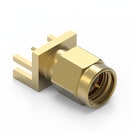 | SPECWR-SMA PCB End Launch, –, – | Simulation– | Availability – | Status Activei| Production is active. Expected lifetime: >10 years. | Product seriesWR-SMA PCB End Launch | – | – | – | – | Operating Temperature -65 °C up to +165 °C | – | Insulation Resistance5000 MΩ | – | – | – | – | – | PackagingTray | Ingress Protection CodeNone | PCB Thickness1.6 mm | Center ContactØ 0.76 | –Check availability | ||||||||||||||||||||||||||||||||||||||||||||||||||||||||||||||||||||||||||||||||||||||||||||||||||||||||||||||||||||||||||||||||||||||||||||||||||||||||||||||||||||||||||||||||||||||||||||||||||||||||||||||||||||||||||||||||||||||||||||||||||||||||||||||||||||||||||||||||||||||||||||||||||||||||||||||||||||||||||||||||||||||||||||||||||||||||||||||||||||||||||||||||||||||||||||||||||||||||||||||||||||||||||||||||||||||||||||||||||||||||||||||||||||||||||||||||||||||||||||||||||||||||||||||||||||||||||||||||||||||||||||||||||||||||||||||||||||||||||||||||||||||||||||||||||||||||||||||||||||||||||||||||||||||||||||||||||||||||||||||||||||||||||||||||||||||||||||||||||||||||||||||||||||||||||||||||||||||||||||||||||||||||||||||||||||||||||||||||||||||||||||||||||||||||||||||||||||||||||||||||||||||||||||||||||||||||||||||||||||||||||||||||||||||||||||||||||||||||||||||||||||||||||||||||||||||||||||||||||||||||||||||||||||||||||||||||||||||||||||||||||||||||||||||||
| Expected Availability | Opening inventory | Quantity |
|---|---|---|
| Current Availability | – | – |