Details
| Topologie | Abwärtswandler |
| Eingangsspannung | 8-19 V |
| Schaltfrequenz | 100-2500 kHz |
| Ausgang 1 | 5 V / 2.5 A |
| IC-Revision | D |
Beschreibung
The TPS65320-Q1 device is a combination of a 40-V, 3.2-A, DC-DC step-down converter and a low-dropout (LDO) regulator. The DC-DC step-down converter, referred to as the buck regulator, has an integrated high-side MOSFET. The LDO regulator also has an integrated MOSFET and a low-input supply current of 28-µA (typical) in a no-load condition. Furthermore, the LDO regulator has an active-low, push-pull reset output pin. To reduce heat, the input supply of the LDO regulator can auto-source from the input voltage to the output of the buck regulator. The low-voltage tracking feature can eliminate the need to use a boost converter during cold-crank conditions.
The buck regulator has a switching frequency range from 100 kHz to 2.5 MHz that provides a flexible design to fix system requirements. The external loop compensation allows for optimization of the converter response for the appropriate operating conditions. A low-ripple pulse-skip mode reduces the no-load input supply current to less than 140 µA.
The device has built-in protection features such as soft start, current limit, thermal sensing, and shutdown because of excessive power dissipation. Furthermore, the device has an internal undervoltage-lockout (UVLO) function that turns off the device at a too-low supply voltage.
Eigenschaften
- Qualified for Automotive Applications
AEC-Q100 Qualified With the Following Results:
-Device Temperature Grade 1: –40°C to +125°C Ambient Operating Temperature
- Device HBM ESD Classification Level 2
- Device CDM ESD Classification Level C4B
- One High-VIN Step-Down Converter 3.6- to 40-V Input Range
- 250-mΩ High-Side MOSFET 3.2-A Maximum Load Current, 1.1- to 20-V Output Adjustable
- 100-kHz to 2.5-MHz Adjustable Switch-Mode Frequency
- Less Than 140-µA Operating Quiescent Current
- One Low-Dropout Voltage Regulator (LDO) 280-mA Current Capability With 28-µA (Typical) Operating Quiescent Current in No- Load Condition
- Input Supply Auto-Source to Balance
- Efficiency and Low Standby Current
- Power-Good Output (Push-Pull)
- Low-Dropout Voltage of 300 mV at IOUT = 200 mA (Typical)
- Overcurrent Protection for Both Regulators
- Overtemperature Protection
- 14-Pin HTSSOP Package With PowerPAD™ Package
REMARK:-1)LO3=1uHinputside inductorreferhttp://www.ti.com/lit/ds/symlink/tps65320-q1.pdfpage no.312) L1=2.2uHinputside inductorreferhttp://www.ti.com/lit/an/slva702a/slva702a.pdf
Qualified for Automotive Applications
-AEC-Q100 Qualified With the Following Results:
-Device Temperature Grade 1: –40°C to +125°C Ambient Operating Temperature
-Device HBM ESD Classification Level 2
-Device CDM ESD Classification Level C4B
-One High-VIN Step-Down Converter 3.6- to 40-V Input Range
-250-mΩ High-Side MOSFET 3.2-A Maximum Load Current, 1.1- to 20-V Output Adjustable
-100-kHz to 2.5-MHz Adjustable Switch-Mode Frequency
-Less Than 140-µA Operating Quiescent Current
-One Low-Dropout Voltage Regulator (LDO) 280-mA Current Capability With 28-µA (Typical) Operating Quiescent Current in No- Load Condition
-Input Supply Auto-Source to Balance
-Efficiency and Low Standby Current
-Power-Good Output (Push-Pull)
-Low-Dropout Voltage of 300 mV at IOUT = 200 mA (Typical)
-Overcurrent Protection for Both Regulators
-Overtemperature Protection
-14-Pin HTSSOP Package With PowerPAD™ Package
REMARK:-1)LO3=1uHinputside inductorreferhttp://www.ti.com/lit/ds/symlink/tps65320-q1.pdfpage no.31
2) L1=2.2uHinputside inductorreferhttp://www.ti.com/lit/an/slva702a/slva702a.pdfpage no.2
Typische Anwendungen
- Advanced Driver Assistance System (ADAS)
- Telematics
- Automotive Infotainment and Cluster
Weiterführende Informationen
Artikeldaten
Artikel Nr. | Datenblatt | Simulation | Downloads | Status | Produktserie | L(µH) | IR(A) | ISAT(A) | RDC max.(mΩ) | fres(MHz) | Montageart | ISAT,10%(A) | ISAT,30%(A) | IRP,40K(A) | Muster | |
|---|---|---|---|---|---|---|---|---|---|---|---|---|---|---|---|---|
 | WE-MAIA SMT Speicherdrossel, 2.2 µH, – | Status Aktivi| Produktion ist aktiv. Erwartete Lebenszeit: >10 Jahre. | ProduktserieWE-MAIA SMT Speicherdrossel | Induktivität2.2 µH | – | – | Gleichstromwiderstand108 mΩ | Eigenresonanzfrequenz45 MHz | MontageartSMT | Sättigungsstrom 12.5 A | Sättigungsstrom @ 30%4.2 A | Performance Nennstrom3 A | ||||
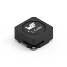 | WE-PDA SMT-Speicherdrossel, 8.2 µH, 5.05 A | Status Aktivi| Produktion ist aktiv. Erwartete Lebenszeit: >10 Jahre. | ProduktserieWE-PDA SMT-Speicherdrossel | Induktivität8.2 µH | Nennstrom5.05 A | Sättigungsstrom5.5 A | Gleichstromwiderstand24 mΩ | Eigenresonanzfrequenz25.2 MHz | MontageartSMT | – | – | – |

