IC manufacturers Intel
IC manufacturers (103)
- All manufacturers
 Analog Devices
 Infineon Technologies
 Microchip
 Onsemi
 Renesas
 ROHM
ROHM STMicroelectronics
 Texas Instruments
- 3peak incorporated (28)
- Ablic (23)
- Acco Semiconductor (1)
- Advanced Power (4)
- Allegro Microsystems (100)
- Alpha & Omega Semiconductor (37)
- AnalogySemi (3)
- AnDAPT Inc (204)
- Anpec (13)
- AXElite (2)
- Backward (6)
- Bright Power Semiconductor (1)
- Broadcom (46)
- Cambridge GaN Devices (18)
- Chipanalog Micro (10)
- Cologne Chips (1)
- Convenient Power (1)
- Dialog Semiconductor (12)
- Diodes Incorporated (259)
- Divimath (8)
- Elmos AG (1)
- EPC (137)
- e-Peas Semiconductors (1)
- Eta Solutions Co. Ltd. (9)
- GaN Systems (8)
- GaNPower (3)
- Giantec (1)
- Gstek Wuxi (1)
- Helix Semiconductor (7)
- IKON (1)
- Indie Semiconductor (8)
- Innovision Semiconductor Inc (2)
- Intel (68)
- Inventchip Technology (3)
- ISSI (51)
- JoulWatt (20)
- KDPOF (3)
- Kinetic Technology (8)
- Lattice semiconductor Corporation (38)
- Littelfuse (1)
- Lumissil Microsystems (8)
- M3 Technology (M3Tek) (7)
- Macnica (22)
- Marvell Semiconductor (1)
- MaxLinear (181)
- Menlo Micro (1)
- MikroE (25)
- MindCet (2)
- Monolithic Power Systems (980)
- Navitas Semiconductor Inc (6)
- NewEdge Technologies, Inc. (1)
- Nexperia (267)
- Nisshinbo Micro Device Inc. (10)
- Novosense Micro (1)
- NXP (335)
- O2 Micro International Ltd (10)
- On Bright (7)
- Panasonic (2)
- PN Junction Semiconductor (2)
- Power Integrations (117)
- Powermat (1)
- Pulsiv (19)
- Qorvo (96)
- Realsil SuRealsil(tek) Microelectronics (1)
- Richtek (297)
- Sanken Electric Co., Ltd. (16)
- Sckipio (6)
- Semtech (86)
- SG-Micro (54)
- SiFive (2)
- Silanna Semiconductor (9)
- Silergy Corporation (33)
- Silicon Laboratory Inc. (108)
- Silicontent Technology (59)
- Silvertel (59)
- Skycore Semiconductors (1)
- Skyworks (33)
- Southchip (14)
- Summit Wireless (1)
- Tagore Tech (7)
- Taiwan Semiconductor (1)
- TDK Corporation (1)
- Tempo Semiconductor (1)
- Torex (37)
- Toshiba (25)
- Transphorm (21)
- TransSIP (2)
- Union (21)
- uPI Semiconductor (2)
- Valens Semiconductor (31)
- Wise Integration (3)
- Wolfspeed (23)
- Xilinx (22)
- XL Semiconductor (3)
- XYSemi (62)
Overview
| Topology | FPGA |
| Input voltage | 16 V |
| IC revision | 1.2 |
Description
The Arria V SoC development board provides a hardware platform for developing and prototyping low-power, high-performance, and logic-intensive designs using Altera’s Arria V SoC. The board provides a wide range of peripherals and memory interfaces to facilitate the development of Arria V SoC designs.
Features
- One Arria V SoC (5ASTFD5K3F40I3) in a 1517-pin FBGA package
- FPGA configuration circuitry
- Active Serial (AS) x1 or x4 configuration (EPCQ256SI16N)
- MAX® V CPLD (5M2210ZF256) in a 256-pin FBGA package as the SystemController
- Flash fast passive parallel (FPP) configuration
- MAX II CPLD (EPM570GF100) as part of the on-board USB-BlasterTM II for usewith the Quartus® II Programmer
- Clocking circuitry
- Si570, Si571, and Si5338 programmable oscillators
- 50-MHz, 66-MHz, 100-MHz, 125-MHz programmable oscillators
- SMA input (LVCMOS)
- Memory
- One 1,024-Mbyte (MB) HPS DDR3 SDRAM with error correction code (ECC)support
- Two 1,024-MB FPGA DDR3 SDRAM
- One 512-Megabit (Mb) quad serial peripheral interface (QSPI) flash
- One 512-Mb CFI synchronous flash
- One 256-Mb NOR flash (EPCQ device)
- One 32-Kilobit (Kb) I2C serial electrically erasable PROM (EEPROM)
- One Micro SD flash memory card
- Communication Ports
- One PCI Express x4 Gen1/Gen2 socket
- Two FPGA mezzanine card (FMC) ports
- One USB 2.0 on-the-go (OTG) port
- One Gigabit Ethernet port
- Two 10/100 Ethernet ports
- Two SFP+ ports
- Two RS-232 UART (through the mini-USB port)
- One real-time clock
- General user input/output
- LEDs and displays
- Eight user LEDs
- One configuration load LED
- One configuration done LED
- One error LED
- Three configuration select LEDs
- Four on-board USB-Blaster II status LEDs
- Two FMC interface LEDs
- Two UART data transmit and receive LEDs
- One power on LED
- One two-line character LCD display
- Push buttons
- One CPU reset push button
- One MAX V reset push button
- One program select push button
- One program configuration push button
- Eight general user push buttons
- DIP switches
- One JTAG chain control DIP switch
- One board settings DIP switch
- One FPGA configuration mode DIP switch
- One general user DIP switch
- Power supply
- 14–20-V (laptop) DC input
- Mechanical
- 7.175" × 9" rectangular form factor
More information
Products
Order Code | Datasheet | Simulation | Downloads | Status | Product series | Pins | Gender | Type | Variant | Durability | Data rate | PoE | Ports | Tab | Improved CMRR | Operating Temperature | LED | PHY Chip Mode | Mount | Shield Tabs | Samples | |
|---|---|---|---|---|---|---|---|---|---|---|---|---|---|---|---|---|---|---|---|---|---|---|
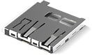 | WR-CRD SD Card Connectors, 8, Socket | Simulation– | Status Activei| Production is active. Expected lifetime: >10 years. | Product seriesWR-CRD SD Card Connectors | Pins8 | GenderSocket | TypePush & Push | Variantwith Card Detection | Durability10 000 Mating cycles | – | – | – | – | – | Operating Temperature -25 °C up to +85 °C | – | – | MountSMT | – | |||
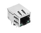 | WE-RJ45 LAN Transformer, –, – | Status Activei| Production is active. Expected lifetime: >10 years. | Product seriesWE-RJ45 LAN Transformer | – | – | – | – | – | Data rate100BASE-TX | PoEnon-PoE | Ports1x1 | Tab PositionDown | Improved Common Mode RejectionNo | Operating Temperature -40 °C up to +85 °C | LED (Left-Right)yellow-green | PHY Chip Modecurrent & voltage | MountTHT | Shield TabsYes |