IC manufacturers (96)
- All manufacturers
 Analog Devices
 Infineon Technologies
 Maxim Integrated
 Microchip
 Onsemi
 Renesas
 ROHM
ROHM STMicroelectronics
 Texas Instruments
- 3peak incorporated (12)
- Ablic (23)
- Advanced Power (4)
- Allegro Microsystems (83)
- Alpha & Omega Semiconductor (37)
- AnalogySemi (3)
- AnDAPT Inc (130)
- Anpec (13)
- AXElite (2)
- Backward (6)
- Broadcom (47)
- Cambridge GaN Devices (16)
- Chipanalog Micro (10)
- Cologne Chips (1)
- Dialog Semiconductor (11)
- Diodes Incorporated (217)
- Divimath (8)
- Elmos AG (1)
- EPC (98)
- e-Peas Semiconductors (1)
- Eta Solutions Co. Ltd. (9)
- GaN Systems (6)
- Giantec (1)
- Gstek Wuxi (1)
- Helix Semiconductor (7)
- Ikanos (3)
- IKON (1)
- Indie Semiconductor (1)
- Innovision Semiconductor Inc (2)
- Intel (80)
- Inventchip Technology (3)
- ISSI (34)
- JoulWatt (20)
- KDPOF (2)
- Kinetic Technology (9)
- Lattice semiconductor Corporation (8)
- Littelfuse (1)
- M3 Technology (M3Tek) (4)
- Macnica (16)
- MaxLinear (175)
- MikroE (7)
- MindCet (1)
- Monolithic Power Systems (878)
- Navitas Semiconductor Inc (6)
- NewEdge Technologies, Inc. (1)
- Nexperia (2)
- Nisshinbo Micro Device Inc. (10)
- Nordic Semiconductor (1)
- Novosense Micro (1)
- NXP (312)
- O2 Micro International Ltd (10)
- On Bright (7)
- Panasonic (2)
- PN Junction Semiconductor (2)
- Power Integrations (96)
- Pulsiv (18)
- Qorvo (86)
- Realsil SuRealsil(tek) Microelectronics (1)
- Richtek (289)
- Sanken Electric Co., Ltd. (16)
- Sckipio (6)
- Semtech (90)
- SG-Micro (19)
- Silanna Semiconductor (8)
- Silergy Corporation (29)
- Silicon Laboratory Inc. (90)
- Silicontent Technology (56)
- Silvertel (54)
- Skyworks (31)
- Southchip (6)
- Summit Wireless (1)
- Tagore Tech (4)
- Taiwan Semiconductor (1)
- TDK Corporation (1)
- Tempo Semiconductor (1)
- Torex (37)
- Toshiba (25)
- Transphorm (21)
- TransSIP (2)
- Union (21)
- uPI Semiconductor (1)
- Valens Semiconductor (18)
- Wise Integration (1)
- Wolfspeed (5)
- Xilinx (18)
- XL Semiconductor (3)
- XYSemi (62)
Analog Devices ADP1853
Synchronous, Step-Down DC-to-DC Controller with Voltage Tracking and Synchronization
Overview
| Topology | Buck Converter |
| Input voltage | 12-18 V |
| Switching frequency | 200-1500 kHz |
| Output 1 | 5 V / 15 A |
Description
The ADP1853 is a wide range input, dc-to-dc, synchronous buck controller capable of running from commonly used 3.3 V to 12 V (up to 20 V) voltage inputs. The device nominally operates in current mode with valley current sensing providing the fastest step response for digital loads. It can also be configured as a voltage mode controller with low noise and crosstalk for sensitive loads.
The ADP1853 can be used as a master synchronization clock for the power system and for convenient synchronization between controllers. The CLKOUT signal can synchronize other devices in the ADP185x family such that slave devices are phase-shifted from the master to reduce the input ripple current, improve EMI, and reduce the size of the input bulk capacitance. The ADP1853 can also be configured as a slave device for current sharing. Additionally, the ADP1853 includes accurate tracking, precision enable, and power good functions for sequencing. The ADP1853 provides a high speed, high peak current gate driving capability to enable energy efficient power conversion. The device can be configured to operate in power saving mode by skipping pulses, reducing switching losses and improving efficiency at light load and standby conditions.
The accurate current limit allows design within a narrower range of tolerances and can reduce overall converter size and cost. The ADP1853 can regulate down to 0.6 V output using a high accuracy reference with ±1% tolerance over the temperature range from -40°C to 125°C.
With a wide range input voltage, the ADP1853 is designed to provide the designer with maximum flexibility for use in a variety of system configurations; loop compensation, soft start, frequency setting, power saving mode, current limit, and current sense gain can all be programmed using external components. In addition, the external RAMP resistor allows choosing optimal slope and VIN feedforward in both current and voltage mode for excellent line rejection. The linear regulator and the boot strap diode for the high-side driver are internal.
Protection features include undervoltage lock out, overvoltage, overcurrent/short circuit, and overtemperature.
Features
- Input voltage range: 2.75 V to 20 V
- Output voltage range: 0.6 V to 90% VIN
- Maximum output current of more than 25 A
- Current mode architecture with current sense input
- Configurable to voltage mode
- ±1% output voltage accuracy over temperature
- Voltage tracking input
- Programmable frequency: 200 kHz to 1.5 MHz
- Synchronization input
- Internal clock output
- Power saving mode at light load
- Precision enable input
- Power good with internal pull-up resistor
- Adjustable soft start
- Programmable current sense gain
- Integrated bootstrap diode
- Starts into a precharged load
- Externally adjustable slope compensation
- Suitable for any output capacitor
- Overvoltage and overcurrent-limit protection
- Thermal overload protection
- Input undervoltage lockout (UVLO)
- Available in 20-lead, 4 mm × 4 mm LFCSP
- Supported by ADIsimPower™ design tool
Typical applications
- Medical and healthcare
- Industrial and Instrumentation
- Telecom base stations
- Intermediate bus and POL systems requiring sequencing and tracking, including
More information
Products
| Order Code | Datasheet | Simulation | Downloads | Product series | L (µH) | IRP,40K (A) | ISAT,10% (A) | ISAT,30% (A) | RDC (mΩ) | fres (MHz) | Material | Samples | |
|---|---|---|---|---|---|---|---|---|---|---|---|---|---|
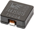 | 744325180 | SPEC | 8 files | WE-HCI SMT Flat Wire High Current Inductor | 1.8 | 22.1 | 7 | 18 | 3.5 | 70 | Superflux |
| Samples |
|---|
| Order Code | Datasheet | Simulation | Downloads | Product series | L (µH) | IRP,40K (A) | ISAT,10% (A) | ISAT,30% (A) | RDC (mΩ) | fres (MHz) | Material | Samples |
|---|